Previous | Next
University of Moratuwa
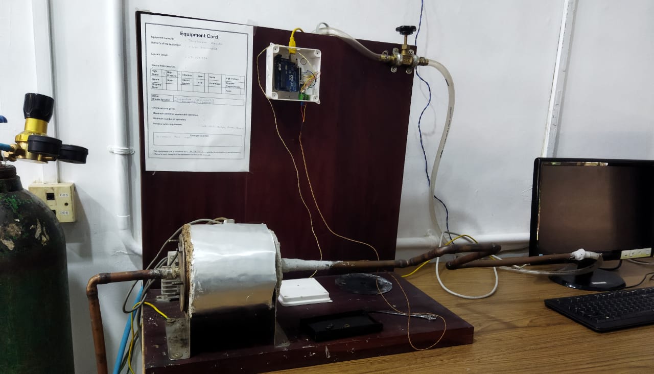
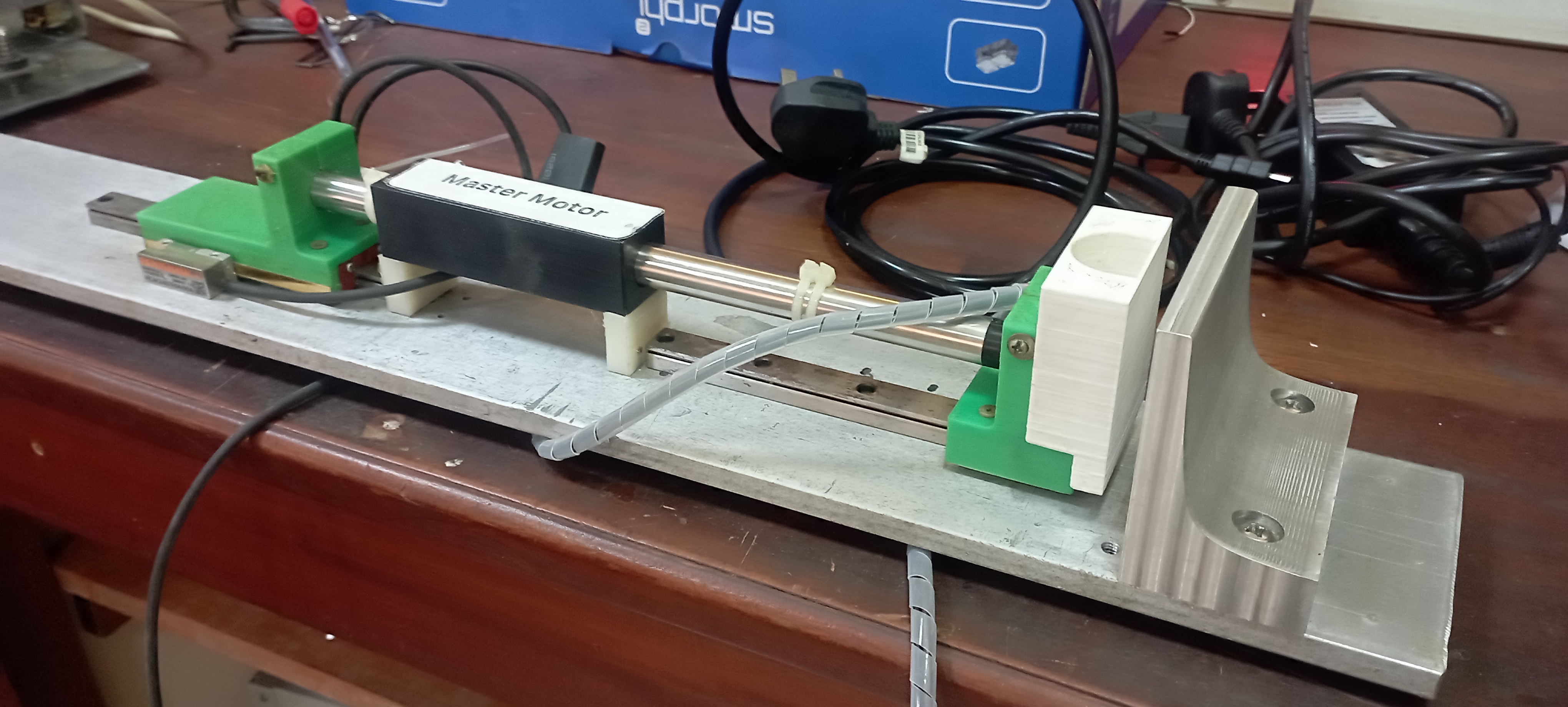
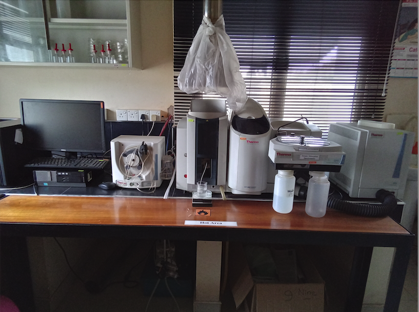
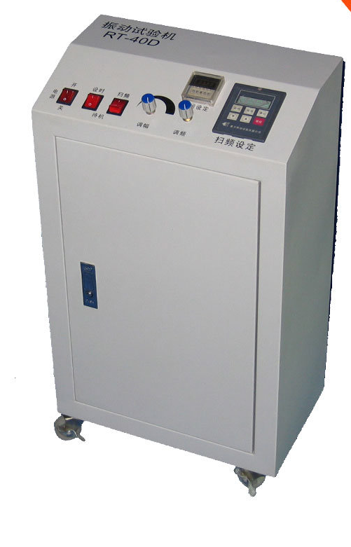
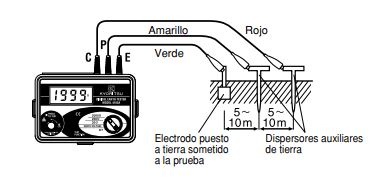
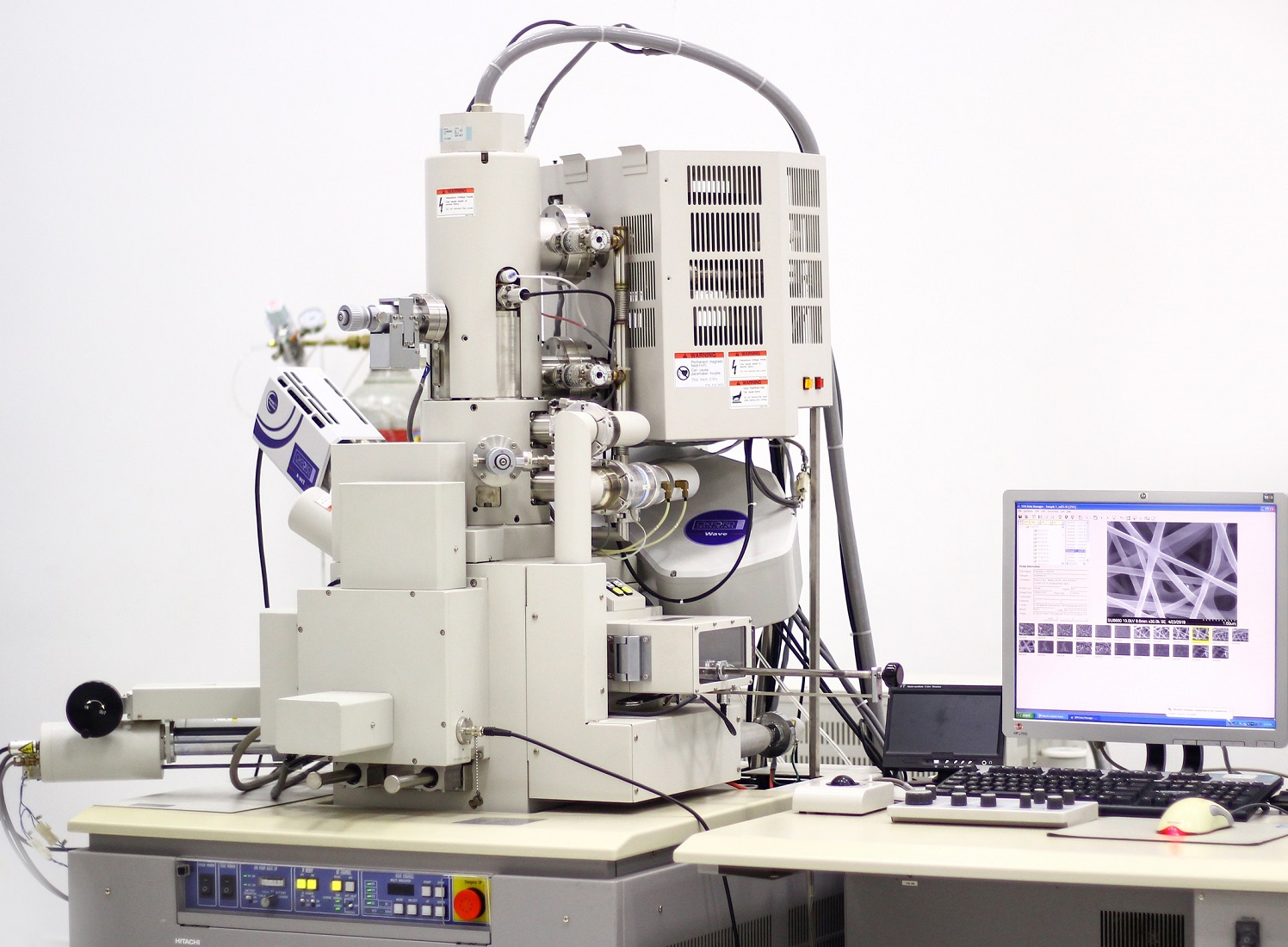
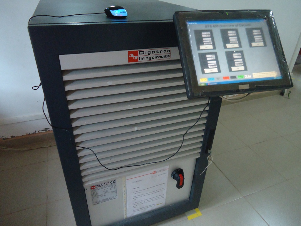
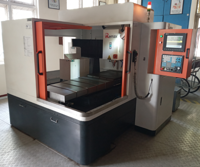
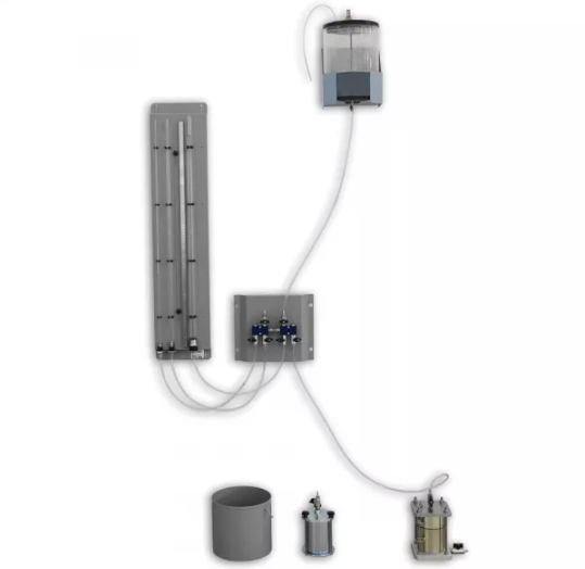
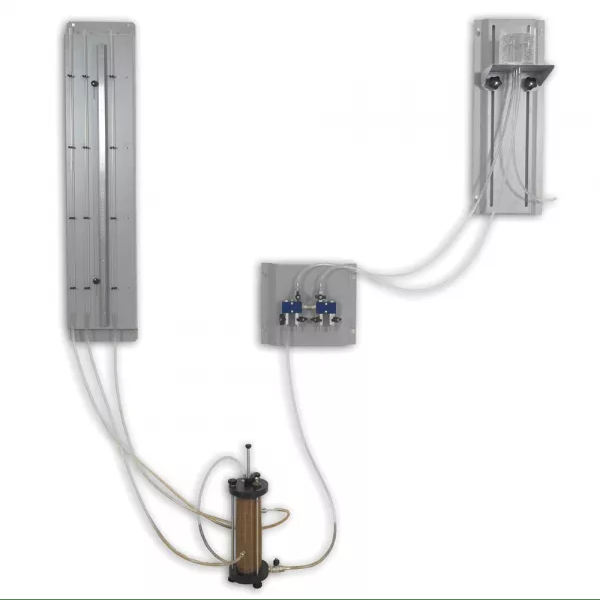
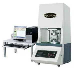
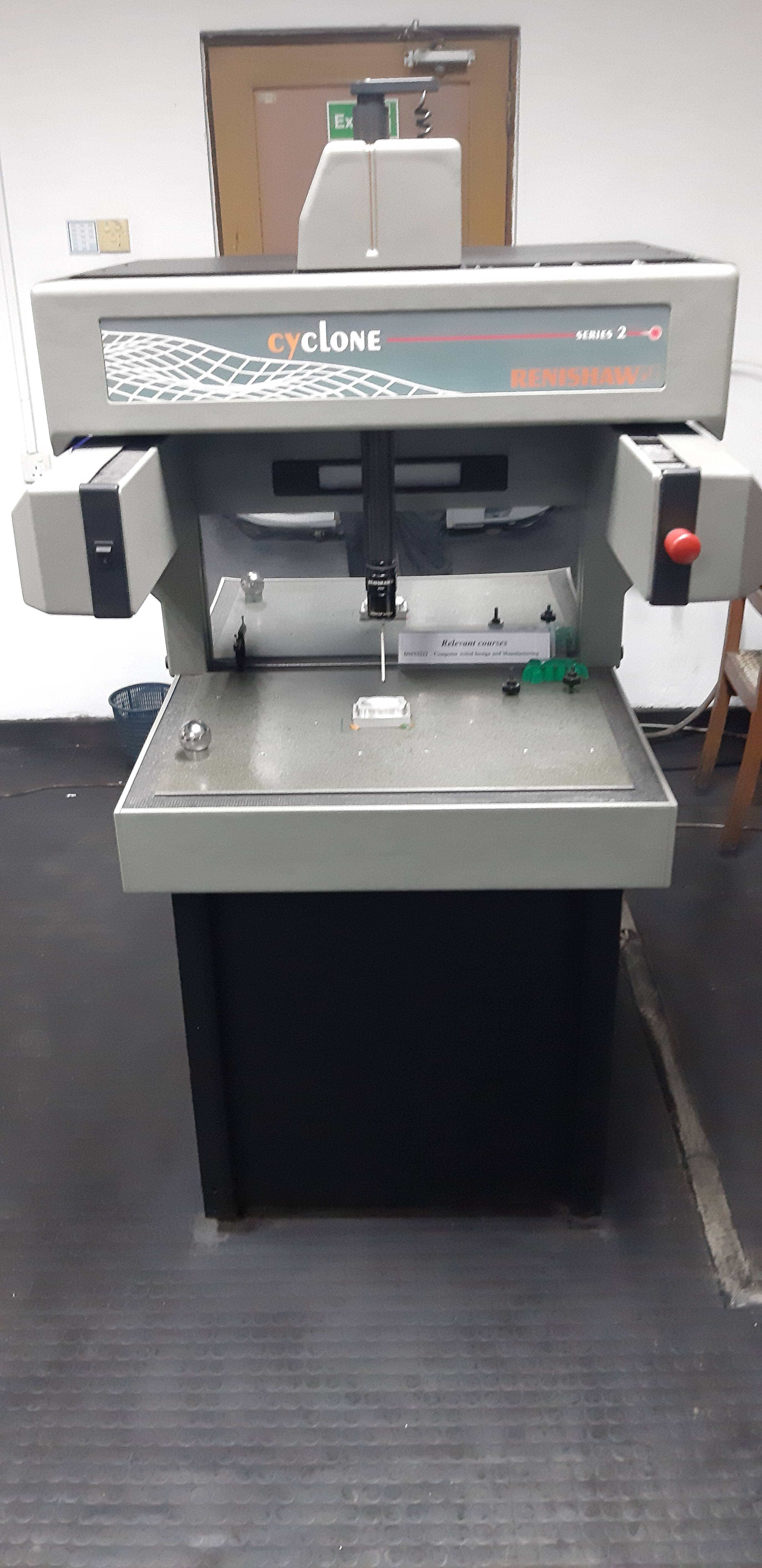
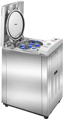
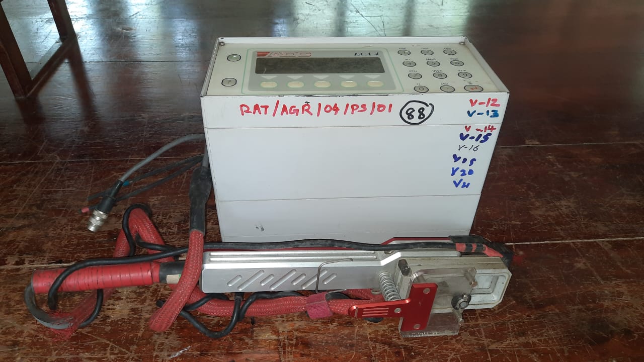
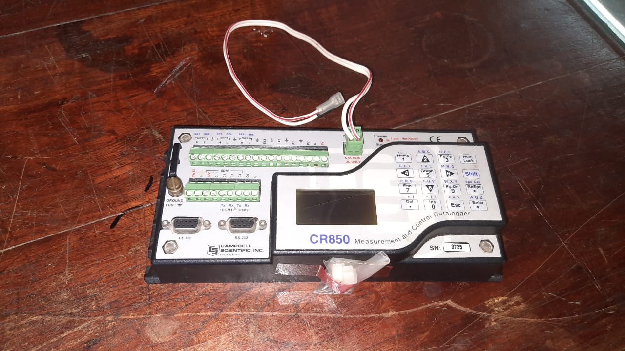
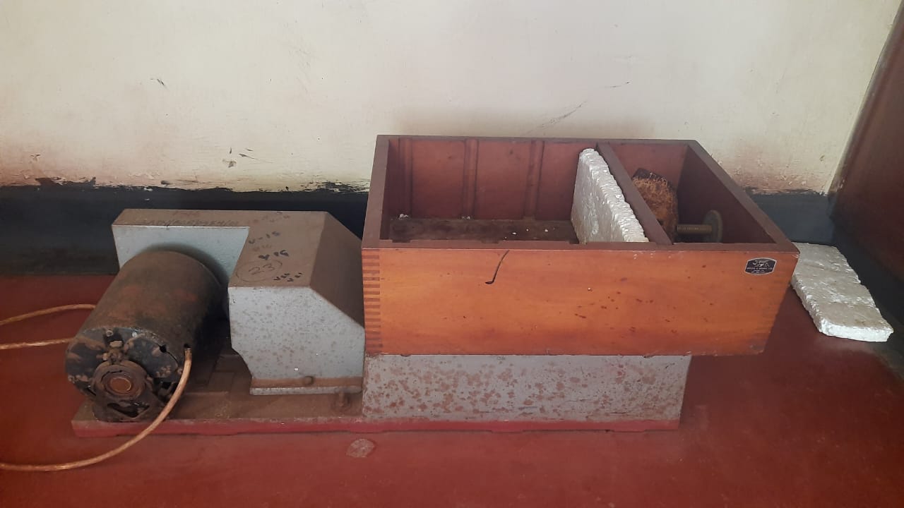
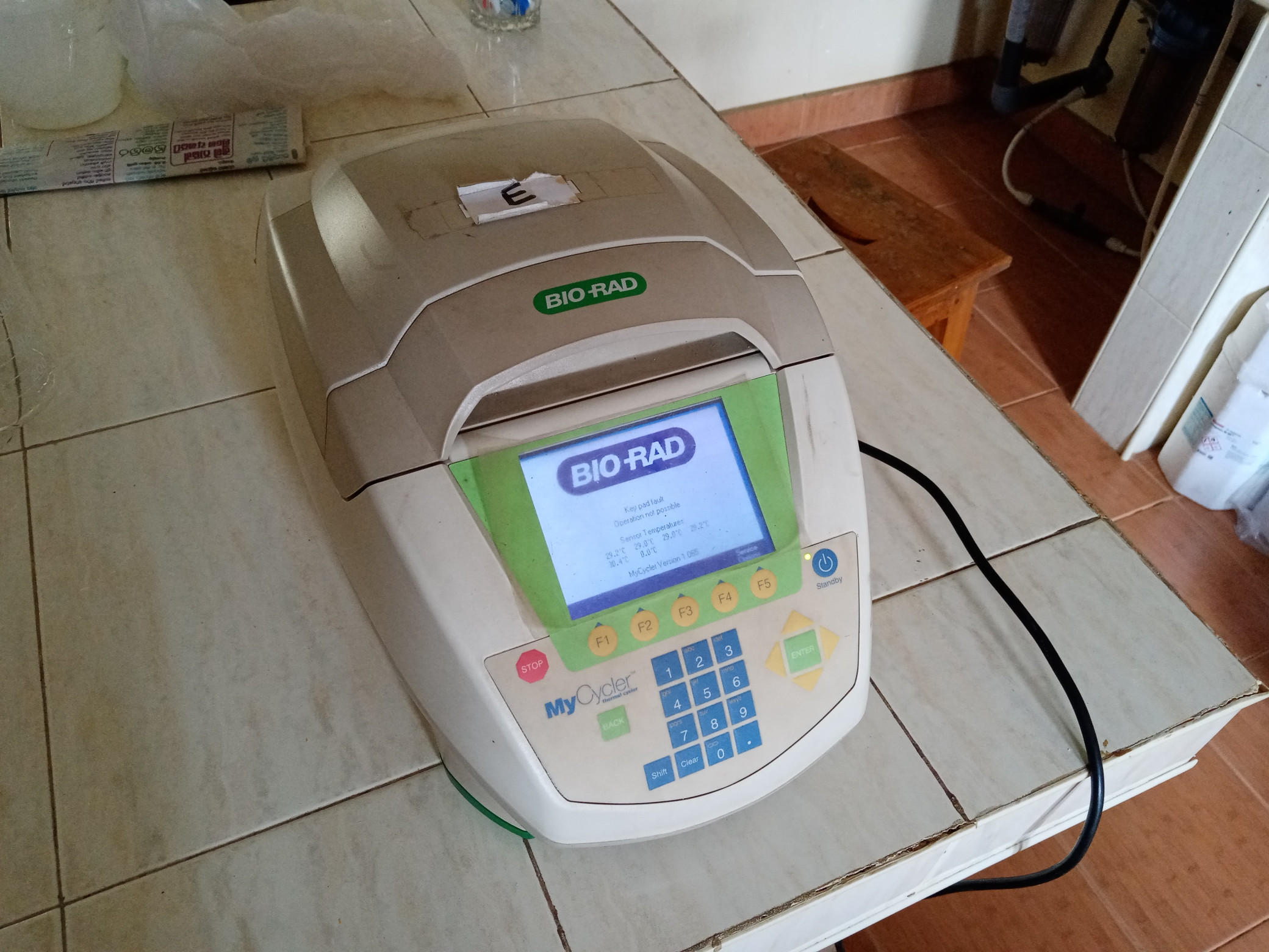
DAQ Card, Multifunction analog/digital I/O | Model 826
University of Moratuwa
-
Faculty: Faculty of Engineering
-
Department: Department of Electrical Engineering
-
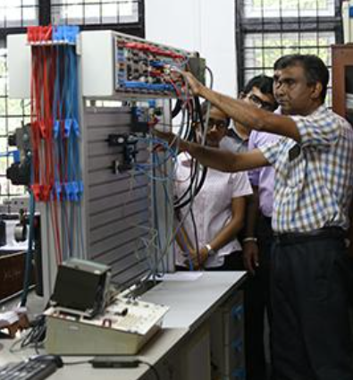
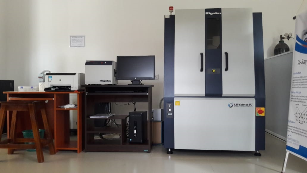
Laboratory : Robotics and Automation Laboratory
Product Category/ Test Name (Matrix):
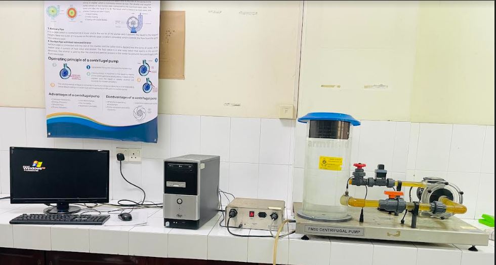
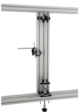
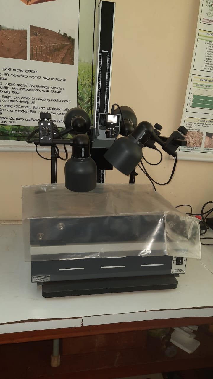
Linear Motor and accessories
Sub Category:
Keywords:
DAQ Card
Service Charge (Rs) - 
.jpg)
.jpg)


.jpg)


.jpg)
.jpg)
.jpg)
.jpg)
1.jpg)
.jpg)
.jpg)
.jpg)
.jpg)
.jpg)
.jpg)
.jpg)
.jpg)
.jpg)
.jpg)
.jpg)
.jpg)
.jpg)
.jpg)
.jpg)


.jpg)
.jpg)
.jpg)
.jpg)

1.jpg)


1.jpg)


.jpg)

.jpg)

.jpg)


.jpg)

.jpg)
.jpg)
.jpg)


3.jpg)


_FN_500P.jpg)

.jpg)
.jpg)
.jpg)
1.jpg)


.jpg)
.jpg)